How to Reball BGA Chips of a Mobile Phones Manually by Hand

Reballing Ball Grid Array (BGA) Chips in mobile phones manually by hand
Reballing BGA chips tends to need and have a good steady hand, since most cellphone technician applied it manually by hands. It also requires good practice  and experimentation before proceeding to reball any chips in mobile phones, because there are chips in mobile phones that can be easily damaged if you are not so familiar of doing it as well.  like the CPU's and the Application processor chips are very vulnerable and can be easily damaged when applying  unrecommended  heat on it. I advice that  spending much time to practice it with non working PC board and chips is a good way to start. To put thing straight up, in real life there are  technician that are good re-baller and some have poor skills on it. that is what I observe mostly when attending many forums on the Internet. The truth is by practicing doing it is the key to enhance re-balling chips skills.

Re-balling Chips Methods
. Prepare the proper Tools -You need to prepare also proper reballing kits and a cleaning kits  for further cleaning the PC board.
 
. A good and controlled hot air temperature, You need to refer to manufacturers manual for proper temperature settings.

Reballing BGA chips manually by hand skill, this tutorial video courtesy of onadbballais


Some technician used IRDA or Infrared Reworks Station and other reballing kit available on the market today. Practice by doing it everyday I assure you can do it yourself within just a few days.

How To Solder SMD Components Manually by Hand

Proper Soldering and De-soldering Methods and Techniques on Surface Mount Components

Soldering is the process of using a metal alloy with a low melting temperature (solder) to Fuse the the electrical contacts of a component to the pads of a circuit board. Proper soldering maximizes the strength and conductivity of the connection. Poor soldering can result in weak connections, higher resistance that causes heat buildup at the connection, and possible failure of the component.

The type of components and the pads to which they will be attached dictate the appropriate soldering method. The correct amount and duration of heat to be applied is a function of the heat transfer characteristics of the component, the circuit board, the solder pads, the solder and flux, and the environment, in which the soldering takes place. For this reason, effective soldering requires reasonably controlled. Some experimentation is usually required to determine the optimal conditions for each application.

General Soldering Guides
All soldering applications require the following considerations:
* Preparation - Clean connections are essential to soldering. Clean connection maximize the ability of the solder to adhere uniformly to the joint surfaces ((welting).
* Soldering Method - The component type and size and your specific application determine the soldering method.
* Materials Selection - The component contacts, circuit board pads, solder,and flux materials must be compatible with soldering method.
* Maximum Temperature - The soldering materials and method determine the temperature profile. All components must be able to withstand the maximum exposure temperature of the soldering operation for specified time and duration.

Manual (Hand) Soldering Technique
While the amount of solder, and the amount and duration of heat to be applied are application-specific, the following general hand-soldering guidelines will lead to consistent and reliable solder connections. A hot air gun is proffered for even heat application and control. The following techniques applies to hand soldering of surface mount components using solder wires and soldering iron.

Preparation
Before beginning to the soldering process, identify the solder composition
and flux type. The solder type dictates the appropriate temperature of the soldering iron tips. Use small diameter wire solder for soldering small SMT components.
Select an appropriate size tip before heating the soldering iron for a fine work result. Clean the tip of any oxidation or contamination. Place a sponge soaked in cold water, nearby for frequent tip cleaning between soldering operations.
Clean the electronic component's contact/leads and the circuit board pads of any contamination or residue.


Hot Air Gun and Soldering Iron Temperature Settings
Hot air temperature temperature tends to be variable when working on any SMD components various Mobile Phones Products used different kinds of solders, check the manufacturer recomendations for specific solder types. The solder manufacturer may only provide the melting temperature range, so you may have to experiment to determine the appropriate temperature.
The amount temperature on Hot Air gun commonly setting is between 250-350 degrees Celsius.
While soldering iron is between 200 to 280 degree Celsius.


This procedure covers the general guidelines for soldering surface mount chip components. The following surface mount chip components are covered by this procedure. While all of these components are different, the techniques for soldering are relatively similar
 

Chip Resistors
The component body of chip resistors is made out of alumna; an extremely hard, white colored material. The resistive material is normally located on the top. Chip resistors are usually mounted with the resistive element facing upwards to help dissipate heat.


Ceramic Capacitors
These components are constructed from several layers of ceramic with internal metallized layers. Because metal heats up much faster than ceramic, ceramic capacitors need to be heated slowly to avoid internal separations between the ceramic and the metal layers. Internal damage will not generally be visible, since any cracks will be inside the ceramic body of the component.
NOTE

Avoid rapid heating of ceramic chip capacitors during soldering operations.

.
Plastic Body
Another style of chip component has a molded plastic body that protects the internal circuitry. There are a number of different types of components that share this type of exterior package. The termination styles for plastic chip component packages vary considerably.

MELF

MELF - Metal Electrode Face cylindrical components. These may be capacitors, resistors, and diodes. It can be hard to tell them apart - since there is no universal coloring or component designators printed on the component bodies.


Replacing SMD Component on Printed Circuit Board 
De-soldering and Soldering Hand Method

TOOLS & MATERIALS


Cleaner


Flux


Microscope or
Magnifying Glass lamp


Solder


Soldering Iron with Tips


Rework Station Hot Air


Wipes


PROCEDURES  TO REMOVE SMD COMPONENT


Add liquid flux to both terminal pad.
Photobucket
Photobucket

Apply Desired Amount of heat on both sides of the leads.
Photobucket
Photobucket

Use a Tweezer to hold the component and observed until the solder joint is melted.
Photobucket
Slowly pull in upward direction, when solders are already melted. do not pull upward forcibly when the solder is not melted yet. You might end up lifted the the terminal surface pads.
Photobucket
 Photobucket


PROCEDURE TO REPLACE SMD COMPONENT

Clean the surface terminal pads with cleaning kits.
Removed remaining old solders by using solder wick
Photobucket
Photobucket

When the pads is cleaned, Apply adequate amount of flux into the pads.
Photobucket
Photobucket

Then apply both pads with fresh solder with desired heat controlled soldering iron.
Photobucket
Photobucket

Place the component in position and hold it steady with a  tweezers so that the hot air won't push the component out of alignment.
Photobucket
Tack it down and apply heat
Photobucket
Wait a moment for the solder to solidify both leads terminal.
Photobucket
Remove heat and hold the SMD components with tweezer until the heats out and  cool.
Photobucket

Cleaned the surrounding  areas with cleaning kit.
Photobucket

You can practice by doing this with an old and non working cellphone PC Board. The more you do practice the more you will master it. Also observed and always become familiar of Hot air and soldering iron   temperature settings. In my experience various type of cellphones solders have different melting point of the solder leads. There are too soft and there are also hard soldered leads to removed.

How to Find Component Parts on PCB Board?

How to Find Component Parts on PCB Board?

A certain components parts is easy to find with an aide of schematic diagrams. In Nokia Phones finding it was been so easy for they provide a complete and accurate component data on their Schematic Diagrams. While other various mobile phone don't have. Some cellphone technicians find it hard to fix some of mobile phone products for they don't provide schematic diagrams to be available, but many experts and masters can do the job even without schematic diagrams. Experts can rely on their deep knowledge on electronics components and circuits, many of them where electronic engineers and also many of them where professionally skilled by experience and mastered for years. You can be one of them if you follow their instinct but before that they all started from scratch.We are all start from scratch.


Now, let's take up a very simple method on how to find certain electronic component's location  where it is being mounted on a particular PCB Board layouts.
Here's an example of Nokia N70 schematic diagram, Download it here if you haven't a copy yet, and make sure you have Adobe Reader installed on your computer to be able to open it.
If you already  have a copy of this schematic diagram,  open it and scroll it down to the bottom page.
In the bottom page which is the last page you may found this Component Finder Page. see picture below:
Photobucket

On the right side you may find the table of components which is listed in codes like for example, Resistors starts with letter "R" then "mounting code" . next to it on the left is the "pattern codes" which is means the spot point which is scaled by letters and numbers on the PC Board,

Photobucket

On the right side of the page is the layout of all of components with respective codes mark on it. Each component mounted in horizontal and vertical positions.
Photobucket

In both sides on the PCB layout is being scaled by letters and numbers, this is were the pattern codes from the first picture above being produce by combining the letter and number to make the mapping spot point.
The spot point of where these letter and number meets across each other, is the exact location where that certain component is being mounted.
Photobucket

Now let's take a little bit exercise on how to use this methods..
Okay, assuming that we are looking for a certain components on a PCB board.
Let say that we are going to find the 2n2 valued capacitor on RF Section for that phone is having a problem of network signal.

now scroll up the page to RF Section which is on page 9 and find these two 2n2 (2.2nanofarad) valued capacitor  see guide picture below;  Just remember and get the Mounting Code for it is the code were going to use as a guide to to the component finder table of components.

Photobucket


Then after finding it scroll back to the Component Finder page Table of components, then find it on the lists of the components codes like "C7524 is on B9" and "C7573 is on A6"

Photobucket

the next thing again you have to do is to remember and get that code then proceed to the Component Layouts. and scale the spot point of  "letter B and 9" then letter "A and 6" on the scaled on the opposite sides.See picture below
Photobucket

The last part is to scroll it up on the whole component layout on the upper page 10 or on your PC board then spot and mark that component where it is being mounted.
Photobucket

There you go you just found it! congratulation!
Practice it more often,so that you can be familiarize on each component or parts for that certain product. The more often you do it, the more chances you will mastered it. sooner,you can work it alone without even using the schematic diagram anymore.

How to Identify the Line Symbols on Schematic Diagram

Identifying the Specified Tracing  Line Symbols on Schematic Diagram

Lines Symbols on schematic Diagram have different specifications.The lines is the path way of every technician for tracing connections from one component to another components or circuits.
Every lines is being specified for a certain purposed, to let the troubleshooter know of what particular source flows on it, like, positive voltages, negative or ground lines, currents, frequency signals, logic digital signals, clock data signals,etc.
In this lesson we are going to take a brief knowledge on how to identify each specified lines for this is so important when it comes to hardware troubleshooting methods.

Photobucket


Lines Tags and Specifications
Line Specifications is also the basis on how and where that certain  components connects across to another components. In this method, finding and tracing in between line to to line is easy for troubleshooter. This is also helps to identify which particular circuits accompanied by a certain components.
Bundled lines- Its a line composed of many lines being combined into one thick line symbol to indicate that the line is composed of assorted line areas across to it.
Line codes - A label used to identify a line continuation from circuits to circuits.

Photobucket

Integrated Chips also coded with letter and number combination. The line codes specify the bumps or terminal pattern of the chips package.
Photobucket

The line codes is used to determine each bumps or terminal took place on the main chips terminal patterns

Photobucket
A power IC RETU of Nokia Handsets

Learning with Block Diagram on How basically Cell-phone works?

How basically Cell-phone works? 

In this lesson we are going to take a brief familiarization of a typical block diagram of a cellphone.
Block Diagram can help us understand the flow of a certain part of a cellphone's circuit.
A Cell-phone handset is basically composed of two sections,
which is RF and Baseband Sections.
RF
RF refers to radio frequency, the mode of communication for wireless technologies of all kinds, including cordless phones, radar, ham radio, GPS, and radio and television broadcasts. RF technology is so much a part of our lives we scarcely notice it for its ubiquity. From baby monitors to cell phones, Bluetooth® to remote control toys, RF waves are all around us. RF waves are electromagnetic waves which propagate at the speed of light, or 186,000 miles per second (300,000 km/s). The frequencies of RF waves, however, are slower than those of visible light, making RF waves invisible to the human eye.


Baseband
In signal processing, baseband describes signals and systems whose range of frequencies is measured from zero to a maximum bandwidth or highest signal frequency. It is sometimes used as a noun for a band of frequencies starting at zero.
In telecommunications, it is the frequency range occupied by a message signal prior to modulation.
It can be considered as a synonym to low-pass.
Baseband is also sometimes used as a general term for part of the physical components of a wireless communications product. Typically, it includes the control circuitry (microprocessor), the power supply, and amplifiers.
A baseband processor is an IC that is mainly used in a mobile phone to process communication functions.

Basically Baseband also composed of to sections which is the Analog and Digital Processing Sections. So, we are going to separate each other for better and easier to understand.
Cell-phone have three different sections which is the following.
I prepare this to be simple and easy instead of using or explaining it with deep technical terms .
In this manner, it is easy for us to understand the concepts and methods of how basically the cellphone works.

Cell-phone have three sections since baseband is differentiated by into two which is the Analog and Digital function while the RF section remains as a whole circuit section.. which is the following cosists.
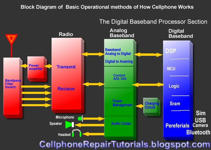
1. Radio Frequency (RF Section)
2. The Analog Baseband Processor
3. And the Digital Baseband Processor. 


Photobucket

Radio Frequency Processing Section
The RF section is the part of the cell-phone circuit is also known as RF Transceiver.
It is the section that transmit and receive certain frequency to a network and synchronize to other phone.

The RF - A radio section is based on two main Circuits.
1 Transmitter
2 Reciever

A simple mobile phone uses these two circuits to correspond to an other mobile phone. A Transmitter is a circuit or device which is used to transmit radio signals in the air.and a reciever is simply like radios which are used to recieve transmissions(Radiation) which is spread in the air by any transmitter on a specific frequency.
The two way communication is made possible by setting two transmitters and two recievers sycronized in this form that a trasmitter in a cell phone is syncronised with the frequency of other cell phone's recieving frequency same like the transmitter of second cell phone is syncronised with the recieving frequency of first cell phone. So first cell phone transmits its radiation in the air while the other phone listens it and same process is present in the opposit side. so these hand held two cell phones correspond to one another.
the technology used in these days is a little bit different but it is based on the basic theory prescribed before. the today's technology will be discussed in later on.
Photobucket


Analog Baseband Processor
A/D and D/A section
The analog baseband processing section is composed of different types of circuits.
This section  converts and process the analog to digital (A/D) signals and digital to analog signals (D/A).
Control section 
This is the section acts as the controller of the the input and output of any analog and digital signal.
Power Management
A power management section in mobile phones is designed to handle energy matters that is consumed in mobile phones. There are two main sub sections in a single power section.
• Power Distribution and switching section
• Charging Section
A power distribution section is designed to distribute desired Voltages and currenst to the other sections of a phone. this section takes power from a battery (which is figured commonly 3.6 Volts)and in some places it converts or step down to various volts like 2.8 V 1.8V 1.6V etc.while on other place it also
steps up the voltage like 4.8 V. this section is commonly designed around a power IC(and integrated circuit) which is used to distribute and regulate the voltage used in other components.
The Charging section is based on a charging IC which takes power from an external source and gives it to battery to make it again power up when it is exhausted. this section uses convertibly 6.4 V from an external battery charger and regulates it to 5.8V wile giving it to battery. The battery is made charged by this process and it is ready to use for the next session (a battery session is a time which is provided by the manufacturer of a cell phone for standby by condition of a mobile phone or talk condition.)
Audio Codecs Section
This section where analog and digital audio properties being process like the microphone, earpiece speaker headset and ring-tones and also the vibrator circuits.
Photobucket

Digital Baseband Processor
This is the part where All Application being process. Digital Baseband Processor section is used in mobile phones to handle data input and ouput signal like switching, driving applications commands and memory accessing and executing.
These are the parts and sections o a Digital Baseband Circuit were installed.
CPU
CPU( Centeral Processing Unit) The Central Processing Unit (CPU) is responsible for interpreting and executing most of the commands from the users interface. It is often called the "brains" of the microprocessor, central processor, "the brains of the computer"
Flash and Memory Storage Circuits
*RAM( Random Access Memory)
*ROM,Flash(Read Only Memory
Interfaces such as the following were also part on this section:
*Blutooth
*Wi-fi
*Camera
*Screen  Display
*Keypads
*USB
*SIM-Card

Photobucket


Here a typical overview of a block diagram on latest mobile phone designs.

Various mobile phones have different concepts and design on every aspects, but the methods and operational flow are all exactly the same. It differs on how and what certain IC chips and parts they are being used and installed to a certain mobile phone circuitry.


Photobucket

How to Identify Integrated Circuit Symbols and Layout

Identifying  Integrated  Circuit  Symbols and Layout
Integrated circuits, also called "chips", are electronic circuits where all the components (transistors, diodes, resistors and capacitors) has been manufactured in the surface of a thin substrate of semiconductor material.
Integrated circuit is designed to save extra space on modern electronics.
In electronics, an integrated circuit (also known as IC, microcircuit, microchip, silicon chip, or chip) is a miniaturized electronic circuit (consisting mainly of semiconductor devices, as well as passive components) that has been manufactured in the surface of a thin substrate of semiconductor material. Integrated circuits are used in almost all electronic equipment in use today and have revolutionized the world of electronics.

Photobucket

In mobile phones it is packed with each desired certain applications purpose like
 Power Management, Baseband  Processor, Application Processor , Memory Storage, Audio Codecs, Bluetooth and Wi-Fi Ciruits.

Photobucket
Some large pack chips composed of many circuits and certain application both in-place in one packaging.
IC Chips are very delicate to handle with and troubleshoot if found faulty, it needs a little bit deep knowledge and understanding on how that chips works on a particular circuit. Experience is the best tool to handle with it.

How to Identify DC to DC Voltage Drivers, Regulators and Converters Symbols and Layout

Identifying  DC to DC Voltage Drivers, Regulators and Converters Symbols and Layout

DC to DC Regulators and Converters are packed in a tiny BGA (ball grid array) chips.
It used to convert, regulate and drives a certain amount of current-voltage.
It has the ability to stabilize, reduce or step up a voltage that feeds towards it.
in mobile phones it has a digital signal that been able to switch it on and off.
like for example it switch the LED lamp that used to light up the Display Screen while the cellphone is in used status and turn it off when the cellphone is not in use or at the sleep mode.
Photobucket
There are various kind and designed of these said components which according to each every purpose to the circuit. Sizes and bumps leads also have may differ with each other.

Photobucket

This chips may also damaged cause by a corrosive element or if a short circuit occurs.

How to Identify EMI-ESD Symbols and Layout

Identifying EMI-ESD Symbols and Layout on schematic diagram and PCB board

EMI-Electromagnetic Interference and ESD-Electrostatic Discharge is pack in tiny chips called by many technician as Crystal IC for it glows like a crystal glass. Photobucket
EMI-ESD filter are used to protect a certain circuit from hazardous Electromagnetic Interference and Electrostatic Discharge. 
Electromagnetic Interference cause by elecromagnetic machines like like a chainsaw, an electric blower and other things that has high frequency levels.
Electrostatic Discharge (ESD)- a human body is a potential source of electrostatic and can cause damage, especially to semiconductor devices when touching it.
Photobucket
Photobucket
EMI-ESD Filters can be easily breakdown and busted when those two elements occurs. It often used in Keypads circuit, Display circuit, USB (Universal Serial Bus)Interface circuit, Removable Flash Memory Devices circuit and other Interface that is prone to ESD and EMI hazards.

How to Identify RF Filter Symbols and Layout

Identifying RF Filter Symbols and Layout

RF filters of all types are required in a variety of applications from audio to RF and across the whole spectrum of frequencies. As such RF filters form an important element within a variety of scenarios, enabling the required frequencies to be passed through the circuit, while rejecting those that are not needed.

The ideal filter, whether it is a low pass, high pass, or band pass filter will exhibit no loss within the pass band, i.e. the frequencies below the cut off frequency. Then above this frequency in what is termed the stop band the filter will reject all signals.

Photobucket

Basic types of RF filter

There are four types of filter that can be defined. Each different type rejects or accepts signals in a different way, and by using the correct type of RF filter it is possible to accept the required signals and reject those that are not wanted.

The four basic types of RF filter are:

* Low pass filter
* High pass filter
* Band pass filter
* Band reject filter

As the names of these types of RF filter indicate, a low pass filter only allows frequencies below what is termed the cut off frequency through. This can also be thought of as a high reject filter as it rejects high frequencies. Similarly a high pass filter only allows signals through above the cut off frequency and rejects those below the cut off frequency. A band pass filter allows frequencies through within a given pass band. Finally the band reject filter rejects signals within a certain band. It can be particularly useful for rejecting a particular unwanted signal or set of signals falling within a given bandwidth.

How to Identify Battery Cell Symbols and Layout

 Identifying  Battery Cell Symbols and Layout

A back up battery cell or button cell is being used in cellphones circuit to back up the digital clock crystal oscillator. It used to maintain the clock at its real time status.
Its like when removing the battery of the mobile phone wont reset the settings of the digital clock that is being installed on a phone. Some phones without battery back-up like the old ones need to reset again after removing and replacing the battery. Its a big help to a digital circuits such high tech mobile phones circuit.
A battery cell is have two lead terminal which is negative and positive voltage output.
The metal can case of this type of battery is its positive (+) terminal, and the negative (-) terminal is the cap.
The negative is connected to a ground lines of a circuit while the positive is feed to a clock oscillator circuit. It has low power output voltage range from 1.5 volts to 3.5 volts. In mobile phones used about 3.3voltage output.
They are compact and have long life. They are usually a primary single cell with a nominal voltage between 1.5 and 3 volts. Common anode materials are zinc or lithium. Common cathode materials are manganese dioxide, silver oxide, carbon monofluoride, cupric oxide or oxygen from the air. Mercuric oxide batteries were formerly a common battery type but have been withdrawn from marketing due to their mercury content.
Photobucket

A back up battery may also damaged when due to degradation, corrosion and losses its voltage when being shorted or by liquids like water;
A damaged battery cell can be easily notice when a leakage occurs, its liquid chemical will flow out and can cause damages to a nearby components.
In a mobile phones you can determine when the back-up battery is weak, when try to set the time of the clock, then power it off and by removing the battery for a while and put it back again, when the clock stayed at its time where you set, it means that back-up battery is still working but, if it ask you to set the clock again it means that the back-up battery is not working.

How to Identify Coil Symbols and Layout

Identifying Coil Symbols and Layout on Schematic Diagram.

The symbol of a coil (inductor) is just like a wave lines which emphasized that there is a winding  component on that circuit which means that the coil is connected in there. In cellphone circuit many coil is being used in B+ voltage filtering to avoid saturated voltage and current.
coils are easy to identify in an schematic  diagram for they are form into a wave line. It is labeled with letter "L" which means Inductance.

Photobucket

In cellphone circuit coils are also prone to be easily damaged like when it is being used in B+ line filtering. It will be blown out or end up busted if some short circuit occurs.

How to Identify Power Switch , Mouthpiece, Earpiece and Ringtones Speakers User Interface Symbols and Layout

Identifying User Interfaces Components such as Power Switch, Microphone, Earpiece and Ring-tone speakers and Layouts On Schematic Diagram

User Interface Components are those components
such as power switch, keypads,vibrator , a micro phone such as mouthpiece, speakers like earpiece and ring tones speaker. These components are also important to familiarized with , for these are commonly prone to be easily got damaged. when it comes to hardware troubleshooting, in Nokia service manual or Schematic diagram it is  marked for easy guides while some other various mobile phone products was not.
In the symbols below the power switch labeled as power key, and also likewise the keypad component symbols that is a circle with two pointing lines insides labeled as keyboard.

Photobucket

In mobile phones there is one microphone and two micro speakers being used; First is the microphone that receive   the voice to transmit,
Photobucket
 the two micro speakers are examples on the picture below,
Photobucket

the first one is for the hearing which is called the earpiece, that is the one that send the voice to hear, the second one is for the ring-tones speaker, it is  that send the tones and tell that someone is calling or sending a message. Familiarizing the uses and works of these three micro speakers on a circuit is a big help for troubleshooting.

How to Identify Clock Crystal Oscillator Symbols and Layout

Identifying  Clock Crystal Oscillator Symbols and Layout

Oscillator
An electronic component circuit that have the ability create real time clock signal. a vibrating crystal that made by so-called piezoelectric material produce a maintained and sustained frequency such as applied into real time clock like quartz wristwatches.. This one is being used to maintain the clock system in a digital circuit and maintain Radio Frequency transmitters and Receivers.
It labeled sleep clock oscillator or just clock oscillator in schematic diagrams.
Photobucket

In Cellphones if the clock oscillator is faulty it results on not powering the phone. The phone is dead, because as stated above that  oscillator supports on digital radio  frequencies circuitry.