
How to Read Cellphone's Schematic Diagram?
Schematic Diagram is a layout of symbols and and connection of every electronic components circuit where serve as a guide on how the circuit function or work.
Reading Schematic Diagrams is not a hard task to do, schematic diagrams is a big help to cellphone-repair
especially when working on or tracing lines and finding where a particular components mounted on a PCB board.
Such schematic diagrams is very useful and very important guide in every cellphone technician. It is equivalent to a handbook.
Learn how to read it. At first you might think that it is hard to do so, You are not going to be an experts and master in cellphone repair as long as you don't know how to read it. Many among cellphone repairman exist nowadays that do not have any knowledge about reading it. They always rely on finding free solutions over the internet and forums. Those people who give free solutions are those people who knows how to read a schematic diagram. Now here's your chance to learn and do not rely unto others, and be an expert and master troubleshooter when it comes to hardware problems.
Okay here's a step on how to read a schematic diagrams.
1. You need to download service Schematic Diagrams, as many or complete package in every cellphone products. each unit of a product have specific service diagrams.
2. You need to download Adobe Acrobat Reader so that you can open the schematic file which is in PDF format.
Now assuming that you already have those I've mention above; Let's try to open up one file like for example we are going to open a schematic diagram of Nokia N70.
here's what it looks like when scrolling down all the pages.
Let's take a little brief on each page for simple understanding..
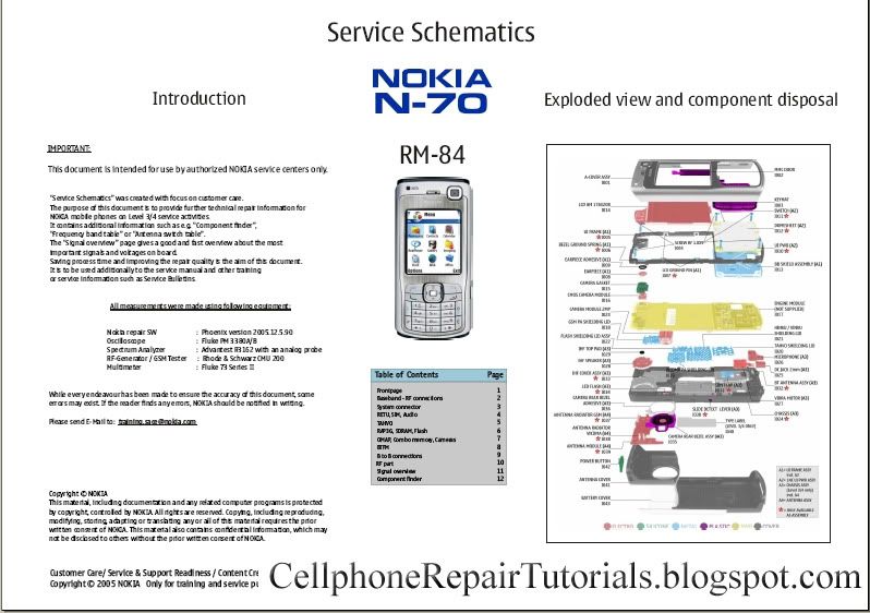
A. page 1, In this page where you can find and Identify the whole assembly of the unit.
this is also where to findd the table of contents of the entire circuit's layouts.
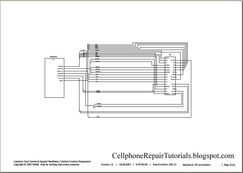
B. page 2, In this page is a block diagram of an RF and Baseband: this is a basic explanation of the entire connection of a circuit. It was called a block diagram for it is being drawed into blocks.
What is a BASE BAND?
In telecommunications and signal processing, baseband is an adjective that describes signals and systems whose range of frequencies is measured from zero to a maximum bandwidth or highest signal frequency; it is sometimes used as a noun for a band of frequencies starting at zero. It can often be considered as synonym to lowpass, and antonym to passband, bandpass or radio frequency (RF) signal.
What is a RF?
Radio frequency (RF) is a frequency or rate of oscillation within the range of about 3 Hz to 300 GHz. This range corresponds to frequency of alternating current electrical signals used to produce and detect radio waves. Since most of this range is beyond the vibration rate that most mechanical systems can respond to, RF usually refers to oscillations in electronics circuits.
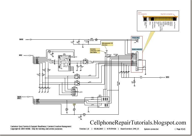
C. page 3, here we can find the system connectors and parts of the unit that correspond to the user or outer parts such us headset, charger and USB connection interfaces.
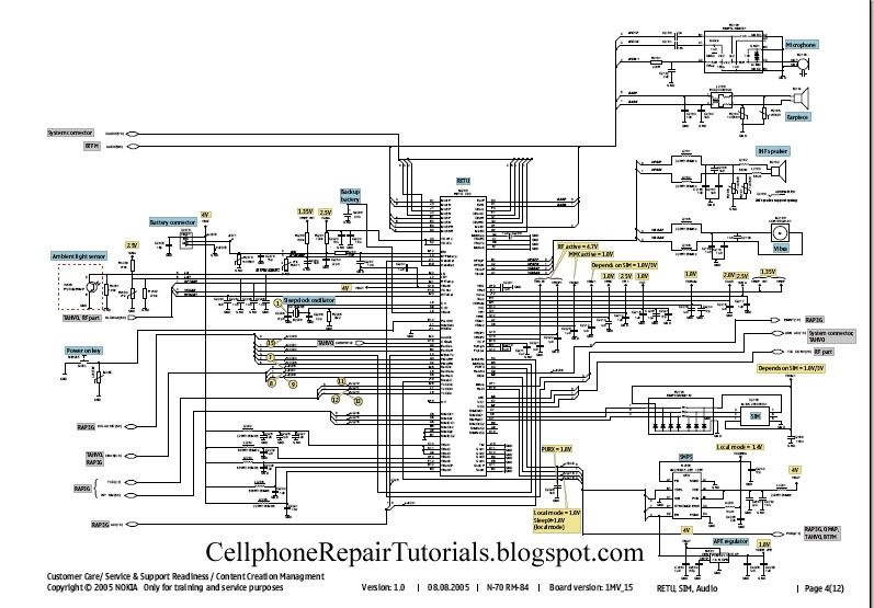
D. page 4, The power management circuit, audio codecs and drivers and the interfaces like the microphone, earpiece, mouthpiece, vibrator, sim-card, battery connections. This is the Power Supply Area of the entire circuits.
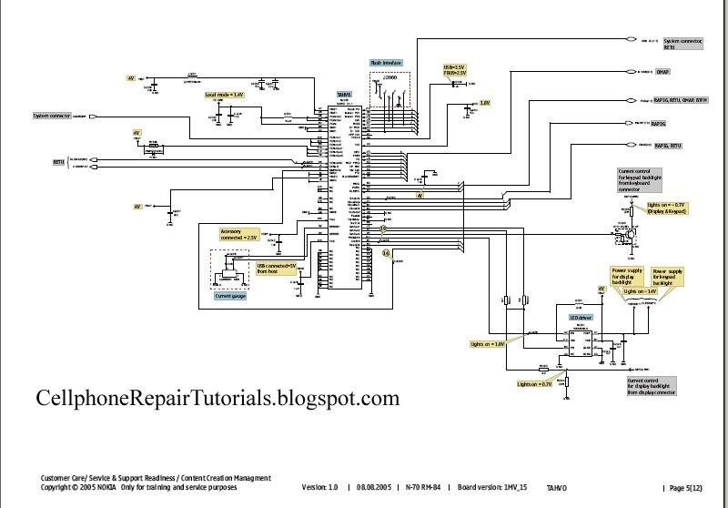
E. page5, Charging Control and Flash Interface Circuit.
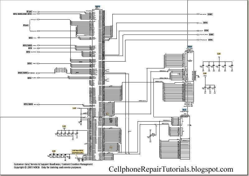
F. page 6, This is the part of the circuit where the all application is being process, Flash IC and memories, this also where application and firmware are being stored.
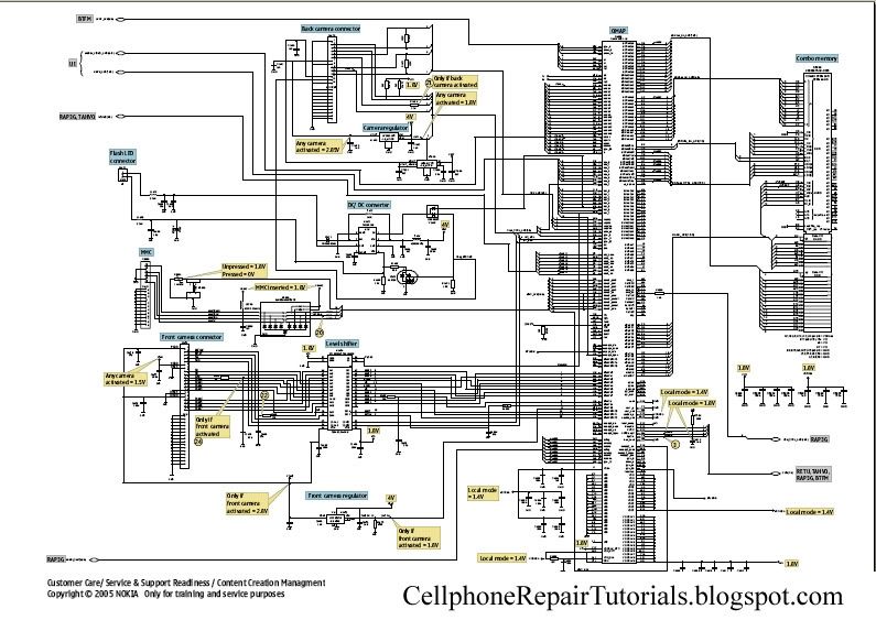
G. page 7, his the Central processing of the unit (CPU) like the personal computer (PC) cellphone also have a CPU to process applications and software.
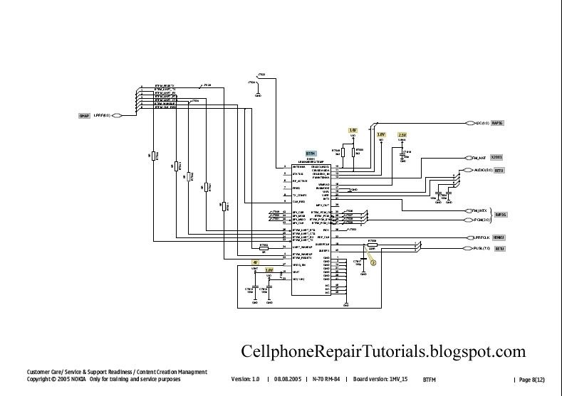
H. page 8, A Frequency Modulation (FM Radio) circuit.
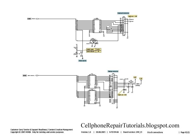
I. page 9,This page is the part of an LCD Display and Keypad circuit.
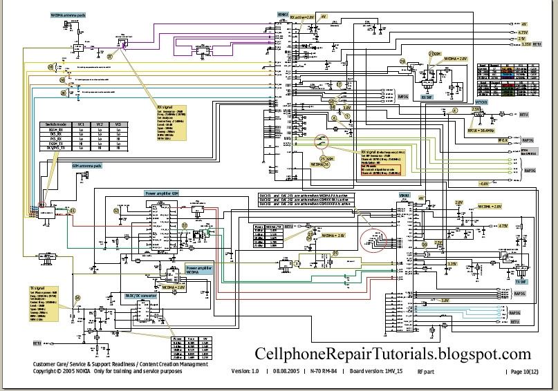
J. page 10, this is the RF components circuit, In this page the RF or the process of a network during Transmitting and Receiving Radio Frequency signals.
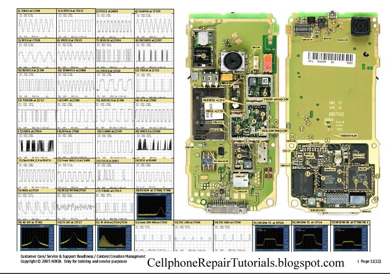
K. page 11, This the structure of the whole PCB Board and all the components mounted in the entire circuit.
this is also where pattern of test-points for check-up during production and servicing.
at the right side is the pattern of waves of frequencies as a guide by using an oscilloscope, frequency generator and spectrum analyzer.
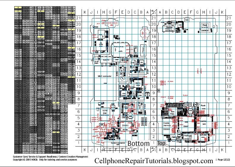
L. page 12, This is where the table of each and every components is mounted on the PCB board written in codes, like Rxxx - resistorr, Cxxx - Capacitor and etc.
The right side is the scale pattern of every components for quick and easy finding it.
that was only the brief explanation of every pages of an Schematic Diagram. Further we will tackle on it even deeper.


1 comments:
thanks so much its i get how working circuit gsm basics knowledge
Post a Comment