Showing posts with label Mobile Phone Repair basics. Show all posts

How to Repair Cellphone Not Charging, No Reponse, Charger Not Supported Problem Issues

There are few types of charging problem issues like Not Charging, No Charging Response and Charger Not Supported.
A problem issues with "Not Charging" shows on a display when a charger is being plug-in, this problem occurs when a required current or voltage is not enough to boost up  and charge the mobile phones battery.
One reason of this problem is  a faulty BSI Line, a BSI line is a Battery Size Indicator that tell the charging control circuit how's the batteries working status.
not%20charging%20response

The battery has a BSI output indicator terminal that connected to its negatives terminal with  desired value of resistor on it.
battery Bsi

One other charging problem issues is the No charging response when a battery charger is being plug-in, it stays no response or nothing happens.
One reason of this is a faulty protection circuit section. this happens when there is no voltage reach to charging circuit indicators and controls. If the protection circuit breakdown this will result to "charging no response" situation. You need to check each components for short and open circuits. You may start from the fuse then to the coil and the diode.
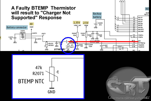
Charger Not Supported problem is cause by a faulty BTEMP thermistor component, BTEMP stands for Battery Temperature, This is the one that monitors the battery temperature status during at charging status, if this one having a problem , it wont allow any charger to proceed to charging stage.
This all, is only a brief explanation of how charging problem issues occurs, while charging the mobile phones .
There are lots of ways on how to troubleshoot each and every kind of handsets. Hope at least, this one let help you understand how charging problem issues occurs, and by this you can gain ideas to move into a stage where you can practice how to troubleshoot this kind of issues.

How to Trace and Map Keypads Layout on Mobile Phone Printed Circuit Board (PCB)

There are few methods in tracing and mapping the keypad layout on a mobile phones keypads on printed circuit board. One of this quick and very easy method is by using an schematic diagram, if that certain mobile phones have available unto it. Schematic diagram is very useful guide in every aspects of hardware troubleshooting.

Now assuming that you already have knowledge how to use and read it, follow this simple steps below.
 Browse to bottom of the pages where yo can locate and find like the picture below., it is the keypad  circuit section. In that schematic layout you will notice that each corresponding key characters is being group into lines. This group of keypad switch lines  is being marked with rows and columns.
  trace each and every lines where those keypads switch symbols is being connected, once you been manage to trace it. configure and trace it on the printed circuit board by using an analog or digital multimeter, just set it the resistance value X1 and attach both probes to corresponding keypads groups in  every rows and column

 keypad layout on PCB board
Practice this kind of method with an aide of schematic diagram, in this way if you're skills grows further, you can then trace any other mobile phones without any schematic diagram available at first hand.

Understanding Keypads Circuit, a way to Learn How to Repair Keypad Problem

Understanding the Keypad circuit may help and boost your knowledge on fixing keypad problem issues on mobile phones. Keypads is a part of user interface being used to navigate or enter numbers, letters and characters, browse application, sends information and etc.

An schematic diagram  below will help us understand how keypad circuits works and which components or parts did this circuit is being connected.
In this diagram the each and every key switching pads is being divided and grouped into rows and columns. Each rows and columns were group into 2 -5 keypads switch. This rows and columns have each corresponding lines according to each and every group of switching pads.


This lines of rows and columns is being filtered for EMI and ESD protection the EMI filter is made of tiny chip that used to protect such EMI and ESD interference.
This rows and columns lines are digital switching signals generated by the application processor to trigger or activate every corresponding digital datas that is being stored and programmed within the mobile phone system memory. This diagram below is an Application Processor that generates and feeds then receives digital data switching signals.
This digital data frequency signals corresponds and interpreted to each key characters that are marked on each keypads. Like for example a combination of row 2 and column 3 will triggered the number 3 when hitting on it.
 this block diagram below shows how the switching signal is being triggered to process a command data.
Various mobile phones have different keypads layouts and specification. A joystick and a volume switch is also parts of keypads switching circuits. Some keypads module designs are made into a flexible wire like those Slide Type package of mobile phones. Some flexible wires are very vulnerable  and common cause of keypad malfunction. 

How Do LED light bulbs works on Mobile Phone Circuit

An LED - light emitting diode is used to illuminate keypads keys and LCD screen displays on all mobile phones handsets. It is being controlled by a voltage or current draws on its terminal leds.
a picture below is an Schematic Diagram that tells us how does the LED circuit works on cellular phone whole circuitry.
On schematic diagram  we notice that the LEDs is driven by an LED driver chip's, and an Switching Control circuit that also being packed in a chip. The LED driver is being used to stabilized the voltage and current and do take control on engaging ON and OFF status of an LEDs to light up or not.
It also drives  the amount  of  brightness or dimming status of the LEDs by applying Pulse Width Modulation signal from the Switching control circuit.

The block diagram below interpreted a component and section or parts of  an LED circuit to work during application process.
The Switching control circuit feeds and release a Pulse Width Modulation Signal (PWM) to switch and light up the LEDs light bulbs. A pulse width modulation signal is a type of digital frequency signal range up to 1khz to enable and implement to take control of  LED brightness.
Once that certain signal is being received by the LED driver, the LED driver now will engage and release the voltage or current that being feeds up from the mobile phones battery supply voltage;
The output voltage release by the LED driver is the one that draws the LED light bulbs to light up.


LED drivers is a high frequency, synchronous boost converter with constant current output to drive up to 5 white LEDs. This device circuit is designed  for maximum safety,  it integrates overvoltage  and short circuit protection when the output is being shorted to the ground. Meaning this chips circuitry will not easily  breakdown for it is designed to protect when short circuit happens.
like for example, the two LED light bulbs commits short circuit to its terminal
In mobile phones application methods; the switching control circuit that release pulse switching signal is also being synchronized programmed by the the application processor (CPU) to engaged a full control on how and which proper situation that the LED will be switch to light up or not.
like for example the LED will only switch and light up, if the handset is being in used and remain off if the handset is not in used.
The above image is an example of the LED circuit, how those particular stages and components being mounted on a phones circuits. Note that the LED driver and switching control circuits is being packed into an Integrated Circuit or ICs.


To all beginners: A bunch of simplified STEP By STEP Procedures On Troubleshooting LED Problem issues on various mobile phones  product will be Posted Here Later.. Just keep on visiting this blog more often.

How Do SIM Card Works on Mobile Phones Circuit

A SIM Card also known as Subscriber Identity Module, A SIM is a Smart Card that can store data from a cellular phone. Those data like identity, location and phone number, network authorization data, personal security keys, contact lists and stored text messages. Security features include authentication and encryption to protect data and prevent eavesdropping.

But how does this SIM card works within the mobile phones circuit? How does mobile phones reads and write data unto it?
In those particular questions above, If we learn answers unto it, we can solve problem issues regarding SIM related problems, like Insert Sim Card and etc.

Now here's a brief explanation on how does SIM Circuit Works on a mobile phones circuit.

A Sim Card have six pads that also corresponds to the six SIM connectors pins, but only five has totally have connection on the entire layout.
SIM DATA - this is a digital data that being stored on a SIM memory
SIM Clock - this is a clock frequency signal that being synchronize to the digital data to create data signal in order transfer or sends and receive data information.
SIM Reset - this is also a frequency signal that triggers or reset all synchronization process.
VSIM B+ Supply Voltage- This a power supply voltage used to activated the SIM circuit.
SIM Ground - a ground line voltage
The other one is not connected

Sim card circuit  block diagram

A Typical block Diagram above shows on how SIM Circuit Works on a Cellular phones circuits.
In the layout the Sim Interface Connector connected directly to SIM Control Circuit. The SIM Control Circuit is the one the generates Clock frequency that triggers the SIM data storage, once the SIM is now being  triggered, it is then now sends data information to the application processor to  begin the process with. The application processor is the one that gathered  all data information from the SIM memory, initiate and activate it, if all information is in desired status.
Those three particular lines of signal flows associated in the circuit shows how the synchronization is being applied. If one of those lines being cut off the sending and receiving process will breakdown, and  will result to SIM problem issues. The Power Supply Voltage through the SIM is also remain stable otherwise a lack of voltage will not activate the SIM to work.


Sim circuit schematic diagram/></a></div><br />
Above an schematic diagram of a SIM Circuit on a <b>NOKIA</b> mobile phone tells us a brief information how a SIM circuit being connected trough the rest of each components.<br />
In <b>Nokia Mobile Phones</b> the Sim circuit is being connected to the <b>Power Management IC</b> then feeds directly also to the <b>Application Processor or CPU</b>.<br />
Some other circuits like the picture below used an <a href="http://cellphonerepairtutorials.blogspot.com/2010/04/emi-esd-filters.html"><b>EMI-ESD</b></a> filtering method, to prevent Electro-magnetic Interference and Electro-Static Discharge damaging the mobile phone

In a picture below an EMI-ESD Filter has been added to protect  the circuit to an Electro-static Discharge and Electro-magnetic Interference disorders. This type of SIM connection circuit is an advantage to mobile phone technician for troubleshooting SIM related problem issues. Thus, type of particular EMI filter is very vulnerable  and mostly create breakdown to the entire SIM connection.
sim circuit schematic diagram 2 /></a></div><div class=
The picture below is an equivalent layout of  an EMI filter and its internal circuitry,
only both frequency and data lines is being filtered.
sim emi-esd filter/></a></div><div class=
The EMI Filter is a tiny chips designed to protect  SIM DATA, SIM Clock and SIM Reset data  signals that flow across trough the SIM connector.
sim
 The EMI-ESD Filter is a highly integrated device designed to suppress EMI(Electromagnetic Interference) and RFI(Radio frequency Interference in a circuit. This filter includes ESD protection circuitry which prevents damaging the mobile phone application when subject to ESD ( ElectroStatic Discharge) surges up to 15 kV.

Here's an example of how the the SIM data signal  flow across the printed circuit board.
Note: this is only shows where the signal flows from component to component connections.

 
 A picture above is an alternative way by many mobile phone technician dealing with SIM problem issues on most Nokia Mobile Phones.

How does Charging Circuit Works from a Battery Charger to charge a Mobile phone Battery

This lesson is also important for charging problem troubleshooting for knowing which parts or components has being used to make a charging circuit. Many mobile phone technicians had been asking me, how does mobile phone charging circuit works? How does a battery charger can charge a mobile phone battery?
To tell the truth many of them has never heard of this even they already fix thousands of mobile phones in their years of cellphone repair careers." and I am one of them.
I don't know but I know how fix it, its so easy"  that's what we've oftenly  said.
Well, we all know that all  mobile phones  are all battery operated handsets that needs to charge the battery so that it will continue working,  failure to charge it will result to unable to power up the mobile phone handsets.

Here's a brief explanation of how charging circuit works,
 I prepare this simple idea and diminished some electronics technical terms so that everyone without adequate knowledge on electronics technical terms might can catch up with this.

A  charging circuit is composed of the following stages or sections. 

1. Battery Charger Circuits - Although this is not found on mobile phones PC board circuit and have separate circuit but definitely  this is also part of charging circuit; without this, the charging circuit is not complete and will not work completely.  
This circuit is all parts and components  that being mounted on any mobile phone charger, this is the one that converts AC (Alternating Current)voltage to DC  (Direct Current)voltage.
What is AC Voltage? This voltage is a power source that we used in our household appliances to work  and operate, this voltage can cause risk of electric shock and very dangerous to humans when being touch.This kind of voltage has an alternate polarity.
What is DC voltage? This voltage is a low level voltage which typically found on any kind of  batteries.
This kind of voltage have two polarities, the negative and the positive.

Here's how the battery charger works, the 110 or 220 AC volts  coming from the electrical outlet at home or etc. will be converted to a desired DC voltage like 4.5 to 6 volt DC because the phone only accepts and can be operated into small amount of DC voltage.


A DC voltage output of a charger is only an artificial DC voltage, why is that? because only a battery cell can produce a 100% pure DC voltage.

2. Protection Circuit- this circuit is composed of a Fuse, Inductor coil Diode and Capacitors,  before the DC voltage reach to the charging voltage control circuits the protection circuit is the one that control and check if that  voltage is in exact amount. Let say the desired amount of DC voltage is only 5.6 volts above that point the fuse will be blown out to stop the voltage to flow so that it prevents damaging to another corresponding circuits.
In a protection circuit below of Nokia BB5 mobile phones a diode is the one that measure the amount of voltage from the battery charger, this diode has a reaching point of desired voltage to measure of how much amount of voltage will be allowed to flow within that line, when exceed to that desired point of voltage the diode will then cut it off.
 like for example if that diode is being designed that only allows only 7 volts from the battery charger to flow on that line. Now, above that desired voltage let say that the voltage becomes 8 or higher the diode will then be reacts and destruct itself, this is what then so-called shorted component; so that the current will flow directly to ground and will not reach to the following or corresponding circuit. If the diode will cut off or shorted the fuse will tends to blow and totally cut the voltage line. The inductor coil's role is to filter unwanted voltage saturation, it rejects abnormal voltage modulation caused by electrostatic interference.

3. Charger Voltage Control Circuit - This is the stage where the charger voltage and current is being stabilized, amplified, rectified, regulated and other voltage purification process is being held in this area before it feeds to the battery. This kind of circuit commonly being pack in a chips together with another circuits. 

A failure of this certain area will result on charging problem status. This area mostly called by most technician as a Charging IC it is because this circuit is inside in a particular IC chips, but eventually  this circuit also accompanied by many other circuit types and not exclusive to a certain charging area.
This pictures shows is the next corresponding circuit from the protection circuit area. The voltage from charger is now then feeds into  three  terminal inputs of the charger voltage control circuits.
in this figure shows  after the voltage stabilization and purification process the voltage is now then feeds to the battery terminal.

4. Charging Control Circuit - this is the area where the charging process is being monitored, this is the one that sends information to  the application processor to start or stop  the charging process. This area is part of  Power management circuit, so-called POWER IC by many technicians.
In this picture  that there are two terminal signal from the voltage  control  that sends data to the Charging control circuit, this two data signals  will inform to the charging control circuit that a charger voltage is being  entered or plug-in. After this charging control circuits receives the data it will then analyze and convert that data into digital signal then sends it to the Application processor.


The application processor which is the brain of all the circuits now then decide if all the data's are in correct or in right information to begin the process,
It always relies on the data that sends by the charging control circuit, then  decide all data and completely process it.


Okay now lets take an example and apply this particular method on a mobile phone circuitry component layout, I have here a Nokia N95 board, which is a good way to start with, while we still working on advance training.  Now, try to analyze and compare all of those previous picture above and combined them into each corresponding stages or section, in this manner you can build an step by step tracing procedure on how to deal charging problem issues.

In the picture above shows, how and where the voltage flow from a charger voltage source through the entire  PC board circuit. This is the the method where you can start and manage how to locate and trace each and every component to find possible problems regarding charging problem issues.

How to Test Mobile phone Speaker,Buzzer or Ringer

Speakers also known as earpiece is the device that allows the handset user to hear the other user during call convesations.
While the Buzzer or a Ringer is the one that sends out the ringtone to be heared by the handset user.
Both Earpiece, buzzer or ringer are same speaker. it only varies the loudness of it sounds being produce.
Ringer buzzer generates more loudness than the earpiece speaker.
A speaker is a device that  converts electrical signal into sounds.
It is made by a magnetic wire winded into a coil and a metal piece of magnet.
below is an example oh how to test of a good and working speakers .

Simply set the analog or digital multi-tester to X1 resistance value, and attach one probe to one the speakers terminal while tick tacking the other one unto it.
A working speaker produce a crackling sounds and the multi-tester pointer moves, while the a busted one will not and have no reading.

How to Test Mobile phone Microphone or Mouthpiece

Mobile phone microphone also known as mouthpiece is the one that intercepts the voice to transmit to other  mobile phone users. Without it or a defective one will result that the other user on a phone cannot hear the one with a defective microphone on its mobile phone handsets.
 A technical term of a microphone is a device used to convert sounds   into electrical  signal.
A microphone is made of an electrical magnetic wire shaped into a round coil with a magnet metal surrounds it,  the mechanical vibration  generated by it will then produce an electrical voltage signal.


Checking the microphone is also been so easy, Just set the analog or digital multi-tester to x1 resistance value then attach both test probe to its terminal. A good sign of a working microphone tends to have a reading while the busted one will have no reading. In some other cases types of microphones may only have a reading to the range of x10 for some high resistance value.

How to test Mobile Phone Charger Voltage

Learning to check mobile phone charger voltage is also a big help when it comes to troubleshooting charging problem.
Various mobile phones have different varieties of charger packaging and designed but almost all of them have one the same operational concepts.

A picture below is an example of a charger used in Nokia Mobile Phones.
The concepts is that the positive voltage is in the inner side of the connector pin while the negative voltage is in outer side of the pin. Charger voltage range from 4.5 to 6 volts and an average rating of 800 milliAmpere current.
Checking it output voltage will be on its connector pin tips. Just set the analog or digital multi-meter to 10DCV or higher range. and connect both test probe to its corresponding polarities. A good and working charger will get the approximately correct reading while the busted one will get no reading.
Many experts know how to fix mobile phone charger for they know the whole designed of its circuitry inside it, but I'd rather not encourage to the newbies to teach about it because it is so complicated and might result risk of electric shock or any possible accident. It is because that circuit involves AC (alternating current) on it, NOTE: Alternating Current is a dangerous voltage and can kill if not have much knowledge about it.

How to Test Mobile Phone Vibration Motor

A mobile phone vibration is created by a small motor called Vibra motor. when applied by a voltage or current it rotates and the vibration is generated by a small tiny piece of metal attach to its tip.
Mobile phone vibrator motor

Checking this small piece of motor was so very easy just set the analog multi-tester range to X1 in resistance
 settings then connect the both probes to each terminals, polarity doesn't matter here for the motor will rotate clockwise if its in the right polarity. and rotates counter clockwise when not in each corresponding polarity.
A good and working vibration motor will then rotate and a bad or busted one will not.

How to check Mobile Phone Battery Voltage

A good and working battery voltage is approximately 3.7 volts DC(direct current),  below that maximum voltage range the phone will not be able to power on.
Checking the battery voltage by an analog multi-meter is so easy, just set  it to a DC range 10volts then attach the both test probes to each corresponding polarity, positive probe to positive terminal, then negative probe to negative battery terminal. Check the maximum battery voltage reading  3.7 volts.
A battery voltage lower than 3.7 volts can power on the handsets but it shows Battery Low on a screen.
A battery voltage lower than 2 to zero volts will hardly charge the phone and won't power up the phone.

A drain battery voltage approximately down to zero volts will not be able to accept charge when a charger is being plug-in. A drain battery will be shock by a a higher voltage range from 6 to 12 volts for a quick charging point as possible to avoid damaging the battery,  a DC regulated power supply. is the equipment used to shock a drained battery.just connect both probe to each corresponding polarity for a quicker period of time, prolonging it will damage the battery itself. You may ask an experience technician in your neighborhood about this method for assistance and safety guidelines.

Familarization: Components and Parts on Samsung Mobile Phone Handsets

 Here is an example of Samsung teardown again courtesy from phonewreck.
Samsung Omnia Teardown

This device is well built. As such, it was a little bit tricky to take apart. Thankfully, all shielding was clip in and the device’s brains were easily revealed.
omnia1
Notably, this device runs on the Qualcomm 6800A and Marvell PXA312. These devices are connected via a Cypress Dual-Port bridge and have separate Power Management Devices. Note that this PCB is impressively packed and impressively small! Another thing to point out is the presence of an SMSC USB PHY. We’ve seen these devices on a variety phones we’ve ripped apart.

Familarization: Components and Parts on iPhone Mobile Phone Handsets

An apple iphone 3GS teardown and analysis is also a big help on overviewing what inside on it.

Apple “surprised” us early this month with the announcement of it iPhone 3G “s”. Whenever Apple releases a new device – everyone and their brother/sister has to get involved.
Dr. Wreck is no exception and has been working hard with the gentlemen/women over at ifixit to get the skinny on the new device. Without further ado, here we go!

Explosion - courtesy of ifixit
Those Apple Engineer’s really know how to pack a PCB. They’ve managed to fit almost everything onto the “top” of the main logic board. The 3Gs’ PCB makes the 3G’s PCB look sparse (the apostrophes were probably a little bit confusing there).
logicboardPCB
Let’s take a minute here to talk about the new Applications Processor Core. Apple has chosen to go from the ARM 11 Samsung S3C6400 to the ARM A8 Samsung S5PC100 with this device.


iPhone 3Gs Block Diagram - In Progress
This is the single largest difference between the 3G and the 3Gs. Firstly the manufacturing process has been chopped from 90nm to 65nm. Pipeline depth has been boosted to 13 – stage from 8. More importantly the clock speed of this newer processor rolls in at 600MHz – opposed to the 412MHz core of the old – obsolete :) 3G. Samsung has also doubled the quantity of L1 cache from 16 to 32KB.
None of this even takes the new PowerVR graphics core into consideration. Apple is clearly thinking along the lines of a gaming device for this puppy. The SGX is fully programmable – like the graphics card on your PC or mac. Expect some sweet gaming action in the near future.
@ 200MHz the SGX can pop 7M triangles/second and render 250M pixels/sec. That’s roughly 7 times the performance of the old, “obsolete” MBX.
It’s kind of like comparing your old 486 to a Pentium.

Logic1

Let’s take a minute here to talk about the new Applications Processor Core. Apple has chosen to go from the ARM 11 Samsung S3C6400 to the ARM A8 Samsung S5PC100 with this device.
iPhone 3Gs Block Diagram - In Progress
This is the single largest difference between the 3G and the 3Gs. Firstly the manufacturing process has been chopped from 90nm to 65nm. Pipeline depth has been boosted to 13 – stage from 8. More importantly the clock speed of this newer processor rolls in at 600MHz – opposed to the 412MHz core of the old – obsolete :) 3G. Samsung has also doubled the quantity of L1 cache from 16 to 32KB.
None of this even takes the new PowerVR graphics core into consideration. Apple is clearly thinking along the lines of a gaming device for this puppy. The SGX is fully programmable – like the graphics card on your PC or mac. Expect some sweet gaming action in the near future.
@ 200MHz the SGX can pop 7M triangles/second and render 250M pixels/sec. That’s roughly 7 times the performance of the old, “obsolete” MBX.
It’s kind of like comparing your old 486 to a Pentium.
Logic1

Bottom of PCB - WiFi/Bluetooth Combo

Familarization: Components and Parts on HTC Mobile Phone Handsets

Here is another teardown and analysis of one of HTC mobile product.


The Touch Pro is a smartphone developed by HTC as a part of their "Touch" line. It is a QWERTY-variant of their Touch Diamond
Other Names: HTC Fuze (AT&T)


Product Features; Specifications


Technical Specifications

Operating System Windows Mobile 6.1 Professional w/ TouchFLO 3D User Interface
Network Support GSM/GPRS/EDGE/HSDPA, UMTS: 900/2100MHz, GSM: 850/900/1800/1900MHz; (operator-dependent)
Screen 2.8" VGA (640 x 480px), 65k Color TFT
Input Method Resistive Touchscreen, Slideout 5-row QWERTY Keyboard, Front Arrow Button Navigation
Wi-Fi 802.11b/g
GPS GPS capable
Bluetooth Bluetooth v2.0 +EDR
Camera 3.2MP Camera with auto focus, VGA CMOS secondary camera
Storage Internal 512MB Storage, External MicroSDHC Slot
Connection Ports ExtUSB 2.0 Hi-Speed (Mini-USB compatible for data-transfer, charger, audio port, and TV-Out)
Physical Attributes Dimensions: 102mm x 51mm x 18.05mm, Weight: 165g with battery
Extra Features FM Radio with RDS

Media Support

Audio Support Codecs: MP3/WMA/AAC+/WAV/AMR-NB


Bill of Materials (CDMA)

* denotes best educated guesses
Processor Qualcomm MSM7501A @ 528MHz
Screen 2.8" VGA LCD, 65k Color TFT
Resistive Touchscreen IC Epson D7741B1 F872U53*
Storage Samsung MCP - NAND Flash + RAM
USB PHY SMSC USB3316
Wi-Fi Texas Instruments WL1251B
Bluetooth Texas Instruments BRF6350BL
GPS Integrated into Baseband Processor
Audio Integrated into Baseband Processor
Accelerometer Kionix KXSD9
RF Transceiver Qualcomm RTR6500 Quad-band GSM/Tri-band UMTS*
Power Management PMIC: Qualcomm PM7540
Power Amp (CDMA-850MHz): Anadigics AW6331R
Power Amp (CDMA-1900MHz): Anadigics AW6332R
Power Amp (Wi-Fi): Texas Instruments WL1251FE

Block Diagram


Teardown Pictures


Source