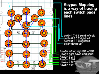
There are few methods in tracing and mapping the keypad layout on a mobile phones keypads on printed circuit board. One of this quick and very easy method is by using an schematic diagram, if that certain mobile phones have available unto it. Schematic diagram is very useful guide in every aspects of hardware troubleshooting.
Now assuming that you already have knowledge how to use and read it, follow this simple steps below.
Browse to bottom of the pages where yo can locate and find like the picture below., it is the keypad circuit section. In that schematic layout you will notice that each corresponding key characters is being group into lines. This group of keypad switch lines is being marked with rows and columns.
trace each and every lines where those keypads switch symbols is being connected, once you been manage to trace it. configure and trace it on the printed circuit board by using an analog or digital multimeter, just set it the resistance value X1 and attach both probes to corresponding keypads groups in every rows and column
Practice this kind of method with an aide of schematic diagram, in this way if you're skills grows further, you can then trace any other mobile phones without any schematic diagram available at first hand.

Custom Search
Blog Archive
Popular Posts
-
Using a multimeter is quite bit difficult for the first time especially the analog type one unlike the digital which is more convenient to u...
-
This is where you can learn a step by step from basic to advance procedure on how to fix major mobile phone handsets problems such as Nokia,...
-
An application processor is a central proccessing unit (CPU) like the one installed on personal computer. It is the brain and controls all k...
-
How to Check Basic Electronic Components Using a Multi-Meter Basic electronic components such as resistors, capacitors, diodes and transi...
-
Odin Flasher Tool for all Samsung Android firmware. The Odin flasher software has been used to manually install Samsung original stock firmw...
Labels
- Advance Turbo Flasher Guide
- Android OS / Windows Mobile Hard Reset Guides
- Android Software Tools
- Apple iPad 2
- Apple iphone
- apple iphone 4
- Apple iPhone Firmwares
- Application Support
- AxeBox Guides
- Blackberry FAQ
- BlackBerry Hardware Repair Guides
- Blackberry MEP Reader
- Blackberry Torch 9800
- Cell Phone Repair Tips
- China Phone Hardware Solution
- China Phone Chips
- China Phone Pinouts
- China Phone Schematic Diagram
- China Phone Tools
- China Phones Flashfiles
- CPF-BOX II Guides
- Cruiser Team Product Guides
- Cyclone Box Guides
- Digi Mic Knopfler
- Disassembling Manuals and Video Guides
- Free Unlocker Software Tools
- Furious Gold Guides
- Google Nexus S
- HTC Hard Reset
- HTC Service Manual
- HTC Software Tools
- Htc Unlock
- Infinity Box Guides
- iPhone Jailbreaking
- iPhone Software Solution
- iPhone Software Tools
- iPod Touch Firmwares
- jaf box repair
- Japanese Phones
- Kyocera Hard Reset
- LG Hard Reset
- LG Firmwares
- LG Schematic Diagram
- LG Software Tools
- Memory card format sofware
- Mobile Phone Codes
- Mobile Phone Repair basics
- MOBILedit
- Motorola Firmwares
- Motorola Hard Reset
- MXKEY Guides
- Nokia Hardware Repair Solutions in EXE
- Nokia IC Datasheet
- Nokia Software
- Nokia 5310 Xpressmusic Repair Guides
- Nokia 5730 Xpressmusic Repair Guides
- Nokia 5800 Xpressmusic Repair Guides
- Nokia BB5 Flashfiles
- Nokia Connectivity Cables
- Nokia DCT3 DCT4 WD2 Flashfiles
- Nokia Flashfiles
- Nokia Hard Reset
- Nokia Hardware Solutions
- Nokia N900 Repair
- Nokia Pinouts
- NOKIA PM /Rpl Files
- Nokia Schematic Diagram
- Nokia Smartphones Hard Reset
- Nokia Software Tools
- Nokia Solutions in shell
- Nokia Spare Parts Compatible
- Nokia X2 Repair Guide
- Odin Flasher
- Online Spare Parts Store
- Sagem Software Tools
- Samsung Flashfiles
- Samsung Hard Reset
- Samsung Service Manual
- Samsung Smartphone OS
- Samsung Tool
- SE USB Driver
- Security Phone Code Reset
- Sharp Schematic Diagram
- Siemens Schematic Diagram
- Smart Phone Software Tools
- Smartphone ROM Firmware
- Software Support
- Sony Ericsson Experia Neo
- Sony Ericsson experia X1
- Sony Ericsson Experia X10
- Sony Ericsson Experia X10 mini
- Sony Ericsson experia X8
- Sony Ericsson Flashfiles
- Sony Ericsson Hard Reset
- Sony Ericsson PlayStation phone
- Sony Ericsson Shematic Diagram
- SonyEricsson FAQ
- Spiderman Box Guides
- Sprint 7700 hardware repair
- Vygis Toolbox Guides
- Z3X Guides
Copyright © 2011 - 2012 Free CellPhone Repair Tutorials | Powered by Blogger


0 comments:
Post a Comment